
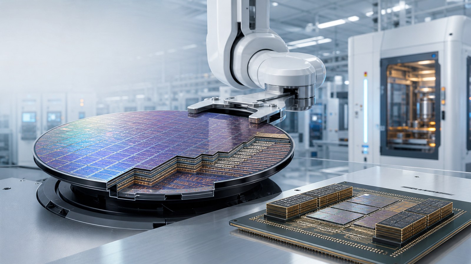
AI chip manufacturing animation turns the journey from silicon wafer to tested accelerator package into a sequence that engineers, investors, customers, trainees, and public audiences can follow without confusing design intent with physical production. A useful animation can show how patterns are built layer by layer on a wafer, how dies are inspected and separated, how logic chiplets and high-bandwidth memory are integrated, and how the finished package is tested before it enters a server.
The goal is not to make semiconductor manufacturing look futuristic. It is to control scale, time, visibility, and terminology so the audience understands what changes at each stage, which steps repeat, and why an advanced AI processor is more than a single square of silicon. That requires a source-driven visual model, carefully chosen abstraction, and review by the people who own the process.
Contact us at info@austinvisuals.com or call (512) 591-8024.
What Is AI Chip Manufacturing Animation?
AI chip manufacturing animation is a visual explanation of how an AI processor moves through design preparation, wafer fabrication, inspection, die separation, advanced packaging, testing, and system integration. It may be a high-level explainer for a public audience, a detailed equipment sequence for sales, a role-specific training module, or a cutaway that shows structures too small, fast, slow, sealed, or hazardous to film.
The phrase covers several different subjects. One project may explain a complete semiconductor value chain. Another may focus on a single deposition chamber, lithography module, wafer-handling system, metrology step, package substrate, thermal interface, or test fixture. Defining that boundary early prevents the animation from becoming a collection of attractive but disconnected cleanroom scenes.
An accurate animation also separates the logical architecture from the manufacturing route. A block diagram can explain compute, memory, interconnect, and input/output. A fabrication sequence explains how devices and metal layers are physically created. A packaging sequence explains how dies, memory stacks, interposers, substrates, and thermal components become a working assembly. Those are related stories, not interchangeable ones.
Why Is AI Chip Manufacturing Difficult to Explain?
The Process Operates Across Extreme Scales
A complete factory is measured in acres, a wafer in millimeters, a package in centimeters, and critical device features in nanometers. A camera cannot preserve all of those relationships in one view. Animation can move between factory layout, tool module, wafer surface, die, transistor layer, package, and board while using visual anchors to keep the audience oriented.
Wafer Fabrication Is Repetitive, Not Linear
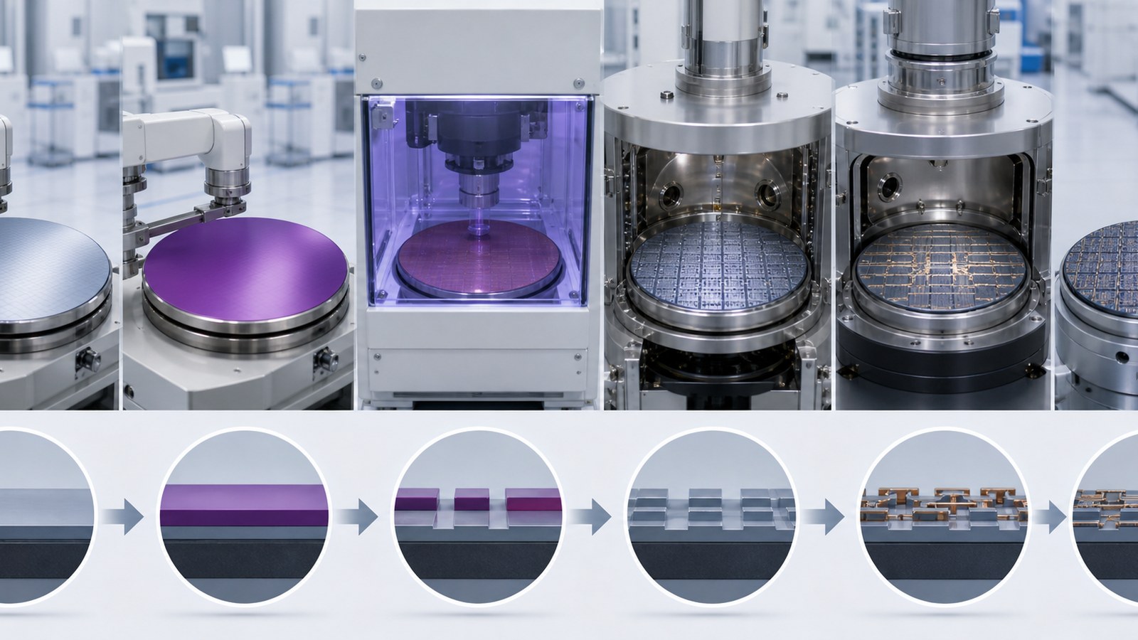
Public explanations often imply that lithography, deposition, etch, cleaning, implantation, and inspection each happen once. In reality, process families repeat as multiple device and interconnect layers are built. The ASML overview of microchip manufacturing notes that chip production involves hundreds of steps. A useful animation shows the repeating logic without forcing viewers to watch every production cycle.
Modern AI Packages Behave Like Systems
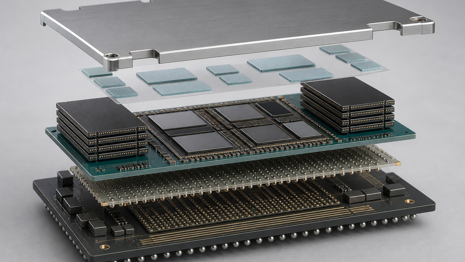
Many high-performance AI products combine multiple compute dies or chiplets with high-bandwidth memory and dense interconnects. The package must support data movement, power delivery, mechanical stability, and heat removal. TSMC describes its CoWoS advanced packaging platform as a foundation for high-performance computing and AI products. An animation should therefore avoid presenting packaging as a decorative casing placed around one finished die.
Completion Has More Than One Meaning
A patterned wafer is not yet a finished product. A separated die may still need electrical classification. A package may be assembled but not validated. A board may operate at room temperature but fail a thermal or signal-integrity requirement. Clear state language helps viewers distinguish fabricated, inspected, known-good, assembled, tested, qualified, and deployed.
Which Manufacturing Stages Can Be Animated?
1. Design Handoff and Mask Preparation
The opening can establish what is being built and which parts of the story belong to design rather than fabrication. Abstract geometry may represent verified layout data, reticles, or mask layers without exposing proprietary circuitry. This is also the right place to state whether the film explains a generic semiconductor process, a specific process node, or a client-owned device.
2. Wafer Preparation and Front-End Processing
The sequence may introduce silicon wafers, cleaning, oxidation, thin-film deposition, photoresist coating, exposure, development, etch, implantation, and planarization. These operations should be shown as process families with defined inputs and outputs. Cross-sections are especially useful because the wafer surface may appear almost unchanged at normal camera scale.
Color can distinguish semiconductor, dielectric, conductor, photoresist, and removed material, but the palette needs a legend and consistent meaning. A glowing line that represents current in one scene should not become a chemical flow in the next. Visual grammar is part of technical accuracy.
3. Inspection, Metrology, and Process Control
Manufacturing animation should not portray every processed wafer as automatically acceptable. Inspection and metrology scenes can show measurement points, defect review, overlay checks, thickness verification, and process feedback at a level appropriate for the audience. For equipment marketing, the emphasis may be tool architecture and sample movement. For training, it may be state recognition and escalation.
4. Wafer Sort, Dicing, and Die Selection
Electrical testing can identify dies that meet different performance or quality criteria before packaging. The visual can move from wafer map to singulated dies while avoiding the misleading impression that all visible die are identical in outcome. If the real program uses binning, known-good-die controls, or traceability, those concepts should be defined by the client rather than invented by the animator.
5. Advanced Packaging and HBM Integration
This stage may show logic dies, chiplets, memory stacks, interposers, redistribution layers, package substrates, underfill, heat spreaders, and other components. An exploded view can clarify relationships, but it should return to the assembled state so viewers understand the final stack. The distances between layers may be exaggerated for teaching and then labeled as not to scale.
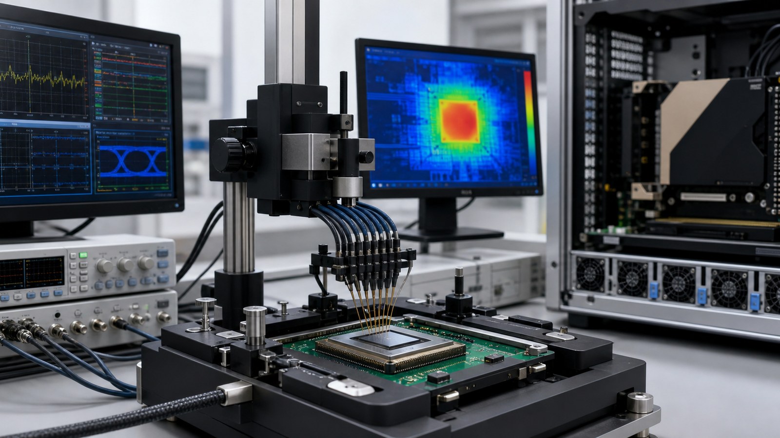
6. Package Test and System Integration
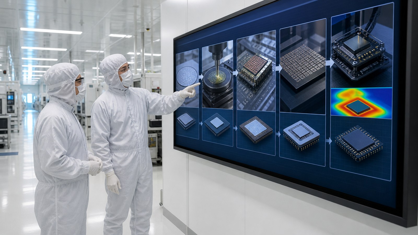
The final sequence can connect component-level testing with the intended application. Socket testing, thermal characterization, signal checks, board assembly, cooling interfaces, accelerator modules, and server installation may all be relevant. The film should stop at the boundary of available evidence; a manufacturing explainer should not imply a performance result that has not been validated.
How Can Animation Support Semiconductor Teams?
Equipment Sales and Technical Marketing
Semiconductor tools are expensive, enclosed, and difficult to demonstrate at a trade show or during an early sales conversation. A semiconductor manufacturing animation can reveal chambers, transfer paths, process zones, service access, and before-and-after states without requiring a live machine. The same controlled master scene can support a launch film, sales presentation, silent trade-show loop, and shorter social edits.
Workforce and Customer Training
Animation can prepare learners to recognize tool states, material routes, component relationships, and decision points before hands-on qualification. It works best as one layer of a training system, paired with approved procedures, instructor guidance, equipment manuals, and practical assessment. It should never substitute for cleanroom certification, lockout requirements, chemical controls, or site-specific authorization.
Investor and Public Communication
A public-facing film can explain why a fab, packaging operation, or new tool matters without disclosing protected dimensions, layouts, recipes, or customer information. The story may focus on value-chain position, production capability, workforce, quality gates, or how advanced packaging supports AI systems. Sensitive and public-safe versions should be planned from the start rather than redacted at the last minute.
Process Alignment and Design Reviews
A low-detail animatic can expose disagreements before final rendering. Equipment engineers may correct a transfer path, package specialists may challenge a layer order, and training owners may identify an omitted decision. The review value comes from making assumptions visible, not from treating the animation as an authoritative simulation.
How Do You Build an Accurate AI Chip Animation?
Define One Communication Job
Start with the decision the audience needs to make. A procurement team evaluating a tool, a technician learning a sequence, and an investor understanding a packaging strategy need different levels of detail. One master model may support several edits, but each deliverable should have one primary audience and outcome.
Create a Controlled Source Package
Useful inputs may include CAD, mechanical drawings, process flow diagrams, package stack-ups, approved cross-sections, equipment photos, interface documents, storyboards, brand standards, safety constraints, and public disclosure rules. Record revision dates and owners. If information conflicts, the animation team should surface the conflict rather than select the most visually convenient version.
Build a State Map Before Detailed Modeling
For every scene, define what exists before the action, what changes, and what evidence confirms the next state. This approach prevents vague transformation effects from replacing the process. It also identifies where time compression, spatial separation, color coding, transparency, or scale exaggeration is necessary.
Separate Literal and Explanatory Visuals
Some shots should resemble the real equipment or package. Others are diagrams designed to explain an invisible relationship. The audience needs to know which is which. Camera transitions, background treatment, captions, and consistent iconography can distinguish a realistic machine view from a conceptual cross-section or data-flow overlay.
Review in Increasing Levels of Fidelity
Approve the script, storyboard, rough layout, and animatic before committing to photorealistic rendering. Subject-matter experts should review the parts they own. A single general approval is not enough when a film crosses wafer process, equipment, packaging, thermal, and system domains.
Protect Intellectual Property
Semiconductor visuals may contain export-controlled, customer-confidential, security-sensitive, or trade-secret information. Define file access, review permissions, reusable assets, public-safe geometry, and final ownership in writing. Generic replacement geometry should be intentionally designed, not produced by casually blurring sensitive details.
What Does AI Chip Manufacturing Animation Cost?
Cost depends on the subject boundary, source quality, number of unique tools or package components, required realism, microscopic cross-sections, runtime, technical-review burden, confidentiality controls, narration, and number of deliverables. A focused animation using client-supplied CAD and an approved process map may be far more efficient than a shorter film that requires reconstructing equipment from photographs or researching an undocumented workflow.
A useful proposal separates discovery, source audit, script, storyboard, modeling, look development, animatic, technical review, rendering, sound, and alternate versions. For broader planning, see Austin Visuals’ guide to 3D animation cost in 2026. A semiconductor project still requires a custom estimate because technical verification can influence the budget as much as runtime.
Why Choose Austin Visuals for AI Chip Manufacturing Animation?

Austin Visuals is a practical fit when a semiconductor or technology story must remain technically grounded while serving people outside the engineering team. We can combine realistic 3D equipment, cutaways, process states, motion graphics, narration, and simplified diagrams in one production without forcing every concept into the same visual style.
Our workflow is built around review gates. We establish the audience and disclosure boundary, organize source files, define the visual state map, and ask technical owners to approve sequence and geometry before expensive finishing. That process is especially useful for equipment manufacturers, AI hardware teams, advanced-packaging suppliers, workforce programs, and organizations preparing material for sales, training, trade shows, investors, or public communication.
Austin Visuals also supports adjacent needs through engineering and technical animation services, B2B 3D animation, and national 3D animation production. The scope can begin with one process explanation and expand into still images, shorter edits, training modules, or a reusable visual library.
Our Clients include:
Conclusion
The best AI chip manufacturing animation does not simply shrink a factory into a cinematic video. It gives every scene a defined state, separates architecture from fabrication and packaging, preserves the difference between explanation and simulation, and invites technical correction before rendering. When those controls are in place, animation can make an exceptionally complex manufacturing story understandable without making it simplistic.
Contact us at info@austinvisuals.com or call (512) 591-8024.
Frequently Asked Questions
What is an AI chip?
An AI chip is a processor designed or optimized for artificial-intelligence workloads such as training or inference. Depending on the application, it may be a GPU, dedicated accelerator, ASIC, FPGA, or another architecture with specialized compute, memory, and interconnect resources.
How are AI chips manufactured?
AI chips move from electronic and physical design into mask preparation and repeated wafer-fabrication processes. Finished wafers are inspected and tested, dies are separated and selected, and one or more dies may be integrated with memory through advanced packaging before final test and system assembly.
How long does it take to manufacture an AI chip?
The answer depends on whether the question includes design, process development, wafer fabrication, packaging, and qualification. Wafer production alone involves hundreds of steps and may take months; a complete new-product program can extend much longer because design verification and manufacturing readiness precede volume production.
Why do AI chips use advanced packaging?
Advanced packaging can combine compute dies, chiplets, high-bandwidth memory, and dense interconnects within one assembly. It helps designers build larger systems from multiple components while addressing data movement, yield, power delivery, and thermal requirements.
What files are needed for an AI chip manufacturing animation?
Typical inputs include approved CAD, package stack-ups, equipment drawings, process maps, cross-sections, photos, interface diagrams, scripts, terminology lists, brand requirements, and confidentiality rules. The exact package depends on the story and disclosure level.
Can animation show microscopic semiconductor processes accurately?
Yes, when the client supplies or approves the process states and layer relationships. Dimensions, spacing, colors, and time may need controlled exaggeration for visibility, and those explanatory choices should be documented rather than presented as literal scale.
Does semiconductor animation replace engineering simulation or work instructions?
No. Animation is a communication and review medium. Qualified engineering analyses, process specifications, equipment manuals, safety procedures, training requirements, and validated test data remain authoritative.